
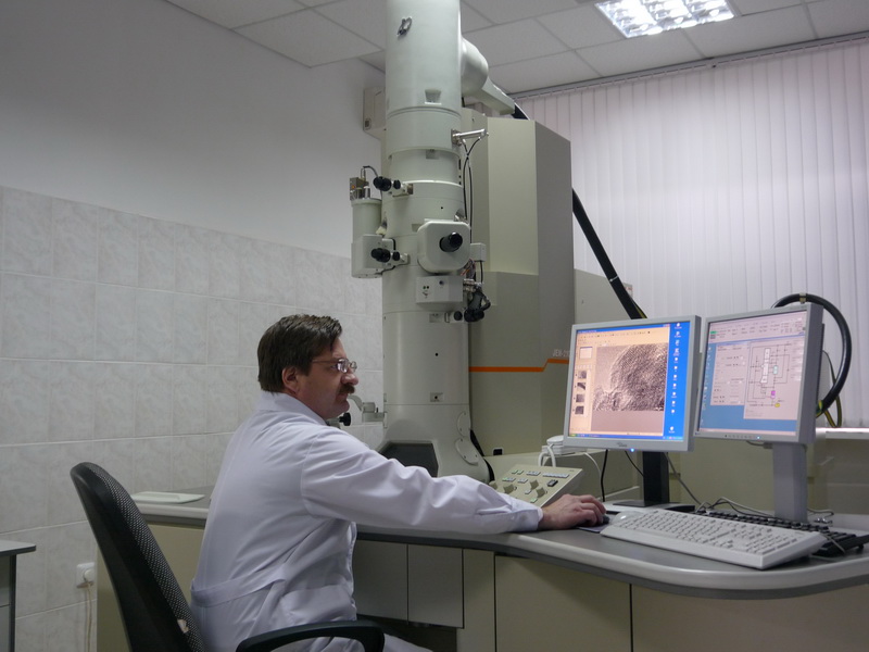
Transmission Electron Microscopy Unit
Transmission electron microscope JEM-2100 produced by «JEOL Ltd.» company (Japan)with STEM-system and energy-dispersive micro(nano)analysis system INCA Energy TEM 350 with crystal X-MAX 80 produced by «OXFORD Instruments Analytical Limited» (Great Britain).
 |
|
Studying the structure of materials, identification of crystalline phases using microdiffraction methods, determination of particles and crystals size, qualitative and quantitative elemental micro (nano) analysis in the point sphere, construction of elements profiles along a given line, mapping the distribution of elements on selected area, mapping diagrams of distribution of elements and phase maps.
Researchers:
- Principal Research Engineer, physicist-mathematician Misevra Sergey Yakovlevich, e-mail: [email protected]
- Research Engineer, doctor of physical and mathematical sciences Alontseva Daria L'vovna, e-mail: [email protected]
- Research Engineer, MEng in materials science Dzhes Aleksey Vladimirovich,
- e-mail: [email protected]
Sample preparation for TEM
 |
 |
 |
| PIPS 691 precision ion polishing system. Preparation of thin films for TEM. | TenuPol-5 automatic electrolytic thinning system. Preparation of thin foils for TEM. | |
Sample preparation:
- Engineer-lab assistant, MEng in materials science Dzhes Aleksey Vladimirovich, e-mail: [email protected]
Scanning Electron Microscopy Unit
Scanning electron microscope JSM-6390LV produced by «JEOL Ltd.» company (Japan) with INCA Energy Penta FET X3 system of energy-dispersive microanalysis produced by «OXFORD Instruments Analytical Limited» company (Great Britain).
 |
|
Study of topography and microstructure of samples and specimens surface (including dielectrics - in low vacuum mode), qualitative and quantitative elemental micro (nano) analysis in the point sphere, construction of elements profiles along a given line, mapping the distribution of elements on a selected area.
Researchers:
- Research Engineer, Master of Physics Sadibekov Aidar Bekadilovich, e-mail: [email protected]
- Research Engineer, PhD in Physics Rusakova Alena Viktorovna, [email protected] e-mail: [email protected]
Sample preparation for SEM:
 |
High precision cutting machine Minitom produced by «Struers» company. |
 |
Grinding and polishing machine LaboPol-5 with a device for automatic grinding and polishing of samples LaboForce-3 manufactured by «Struers» (Denmark). |
Sample preparation:
- Engineer-lab assistant, MEng in materials science Sagidugumar Amangeldi.
X-Ray Diffractometry Unit
X’Pert PRO X-ray diffractometer produced by «PANalitical» company (the Netherlands).
|
Qualitative, semiquantitative phase analysis, determination of the cell parameters and crystals orientation, the analysis of polycrystalline structures, microstress and textures.
Researchers:
- Research Engineer, PhD in Physics , Prokhorenkova Nadezhda Valerievna, e-mail: [email protected].
Mass-Spectrometry and Atomic-Emission Spectrometry Unit
ICP-MS Agilent 7500cx inductively coupled plasma mass spectrometer produced by «Agilent Technologies» company (the USA).
 |
The minimum detectable concentration of the elements
|
Quantitative elemental analysis of inorganic substances and materials (inorganic liquids, water, rocks, ores, metals, ceramics, etc.), isotope analysis.
Agilent 4100 microwave plasma atomic emission spectrometer production of «Agilent Technologies» company (the USA).
 |
The minimum detectable concentration of the elements
|
Quantitative elemental analysis of inorganic substances and materials.
Researcher:
- Research Engineer, Master of Chemistry Polezhayev Stanislav Nikolayevich, e-mail: [email protected]
Sample preparation for mass spectrometry and atomic emission spectrometer:
|
|
Microwave Oven for specimen deterioration Multiwave 3000 produced by «Anton Paar» company (Austria).
The acid deterioration of powder samples for mass spectrometry and atomic emission spectrometry. |

Sample preparation:
- Assistant, bachelor in metallurgy Zabavskaya Anzhela Vladimirovna
X-Ray Fluorescence Spectrometry, Spectrophotometry and Colorimetry Unit
 |
|
Qualitative and quantitative determination of the content (mass fraction) of the chemical elements in solid, liquid and powder samples, rapid analysis of mineralogical, biophysical, biological, environmental objects.
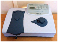
| Spectrophotometer «UNICO-1201» produced by «UNICO» (USA). |
|
 |
|
| Measurement of a transmission coefficients, an optical density and concentration of solutions.
Portable colorimeter DR 890 (HACH 2129) produced by «United Products & Instruments, Inc.» (USA). |
|
 |
|
| Measurement of ions of the elements and organic substances in solution. |
|
| "Alfarad plus" measuring complex for radon, thoron and their fission products monitoring, produced by "NTM-Zaschita" company (Russia). | |
 |
Equivalent volume activity measurement unit:
Volume activity measurement unit:
|
Researcher:
- Research Engineer of the second category, Master of Chemistry Polezhayev Stanislav Nikolayevich, e-mail: [email protected]
Weighing Unit
 |
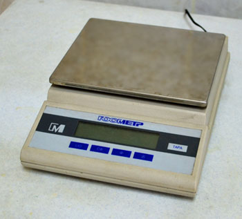 |
| Electronic analytical scales AUM210-I production of «Abbota Corporation» company (USA). | Laboratory scales VLTE-1100 production of LLL "Gosmetr" (Russia). |
| Weighing of samples of up to 210 g up to 0.1 mg. | Weighing of samples and specimens up to 1100 g within the accuracy 0.01g. |
Weighing:
- Assistant, bachelor in metallurgy Zabavskaya Anzhela Vladimirovna
Date of last changes:
16.06.2019